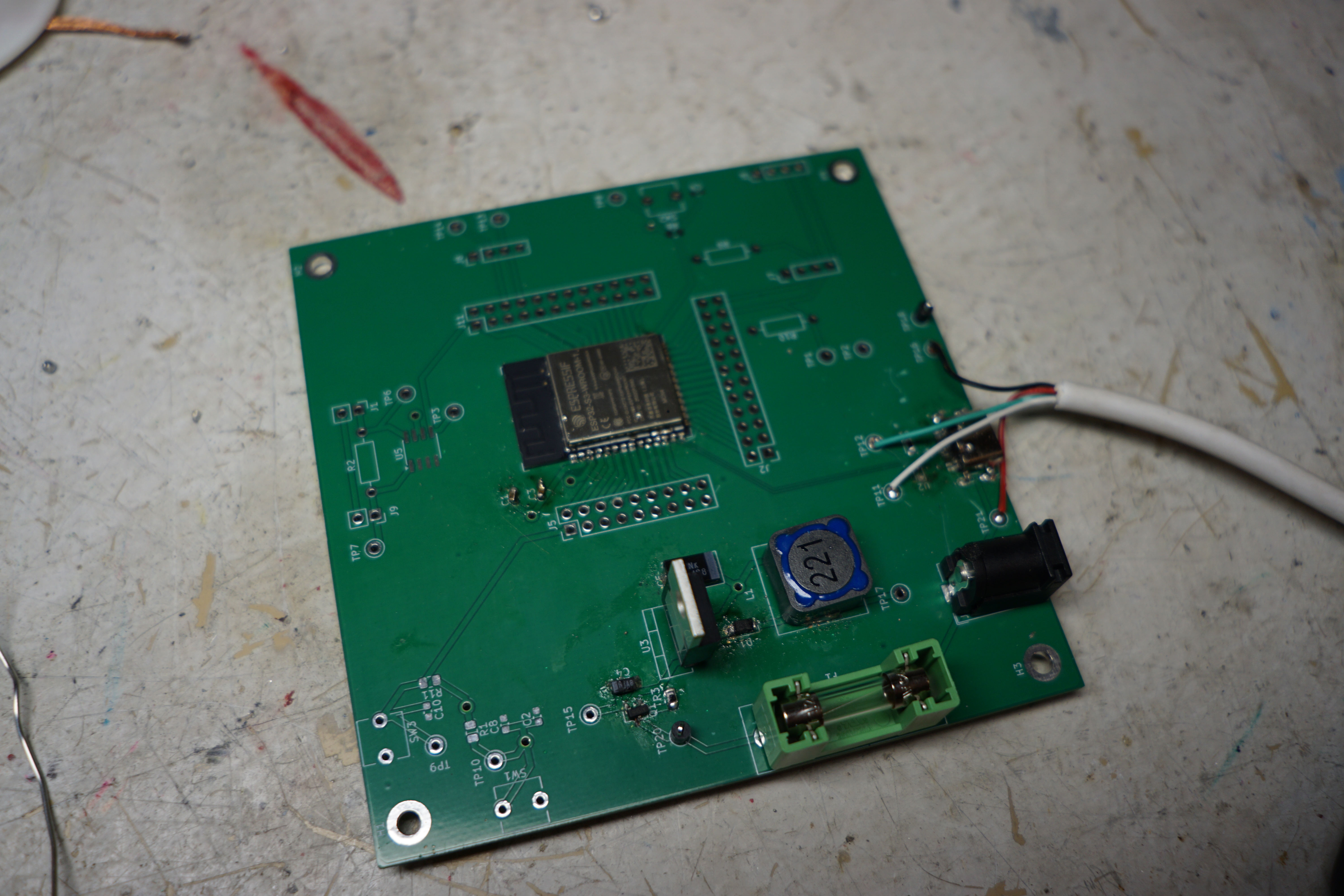
I made a PCB. Can you figure out what I did wrong?
So I made a PCB a couple weeks ago. I spent a lot of time picking parts, designing the schematic, turning the schematic into a PCB, fixing things as they came up and what you see is the result.
So I made a PCB a couple weeks ago. I spent a lot of time picking parts, designing the schematic, turning the schematic into a PCB, fixing things as they came up and what you see is the result.
However, when I got to the assembly and fabrication steps, this is where I found the fallacy in my optimism. From the video you can see that it took me far too long to assemble even only a fraction of my board. I burned several pads off my PCB and destroyed several small parts while trying to attach them. Even though I have been able to recover, I'm looking forward to the next design already to address some of the poor planning that went into this design. The fabrication has taken far too long and I've gotten too frustrated. From the time lapse video you see work over several days with only a limited return.
What are some things that I did wrong?
I used lead free solder, probably at the wrong temperature and without any thing else to compensate.
I'm sorry, but this isn't something I'm going to budge on. I have kids in the house, but it set me back quite a bit. Even using a flux pen, The solder would ball up on the end of my soldering iron, refused to flow to the small surface mount parts, and ended up burning off a lot of copper pads rather than attaching to them. I could have used better rosin / flux, selected more appropriately for the kind of solder I was using. I could have upgraded my soldering iron, and with a better tip and better temperature control, limited the temperatures to only what was needed to get the solder to flow rather than melt all my parts together.
I used built-in footprints for hand-soldered components.
KiCAD is a free, open source, PCB design tool that has come a long way since I first started using it in the 2007-2008 timeframe. It ships with a lot of common parts in its library now, which does make it easier to use. But the fatal flaw here was assuming that the parts that were predesigned were optimized for hand fabrication. Every surface-mount part that I added to my board should have had oversized pads to allow for some imprecision.
Furthermore, in some cases, even though I took care to select parts that proviced access to any leads that I was going to need to solder(no BGA, for example), The footprints that I selected still had no extra buffer around those leads to provide access for hand soldering. These footprints would be compatible with a reflow process, but not hand soldering.
My parts were just too damn small.
I was overconfident in my soldering skills, given all the other issues. My minimum size part for this build was 1206, which is at the lower limit of my soldering capabilities, giving all the other issues listed.
The issue is that just going to through whole components or larger components will not necessarily solve the problem during this early prototyping phase because the supply of those parts is much more limited. It means that I cannot find every part that I want to use.
Another approach would be to hand off some of the fabrication steps to JLCPCB, but in this early phase of prototyping, especially on a budget, that's also not very reasonable.
I think a hybrid approach might still be appropriate if I can solve some of my other issues. If I have to use small parts in certain cases, that is fine, but I certainly did not need to use the smallest surface mount components for capacitors, resistors, and other common components.
pads were too close to other pads or traces.
Even though JLC-PCB produces good boards, in many cases my dwell time that on each pad was too large, causing the solder mask to come off in certain places when the heat was too high, producing shorts that were almost impossible to see or find. So I could have either moved my pads away from other critical traces, or increased the gap between pads and neighboring traces/zones.
I lacked the proper tools
I have a bunch of old equipment including an old soldering iron, passive ventilation, a crappy fixturing device, and poor lighting. My eyes aren't what they used to be, and seeing small features, especially on extra small components, was impossible. In the past, this has not really been an issue because working with larger parts means you can worry less about some of these things. But this was an eye-opening experience that I need to upgrade my setup.
I could use:
- A new pair of helping hands.
- A magnifying glass with light that can be repositioned independent of the helping hands.
- A soldering iron with better temperature control and new fresh tips.
- Better local lighting in my garage.
- Active ventilation to prevent smoke from going up my schnoz.
- A USB microscope or similar that can assist me in identifying parts, finding shorts, and helping me position things.
- I only had one good tweezer, which was infuriatingly bad at holding onto small surface mount parts.
- A better solder sucker.
My USB receptacle was just plain wrong.
First of all, the USB receptacle that I purchased requires the board to have a cutout for the pins to line up, which I didn't pay attention to. Even though the leads were long enough to bend over in order to barely get them to touch the board, they were too narrow and close together for me to be able to solder them effectively without them bridging. I ended up burning off or melting the leads, rendering the parts useless.
Fortunately, I was able to hack an old USB cable to resuscitate the board.
My next design will include through hole pins even if this limits my choices or increases the cost of the part.
Did I do anything right?
Test Points
I provided extra test points throughout the board so that I could use them for fixing broken connections or accessing tough to reach signals.
Jumpers
I disconnected different parts of my circuit using jumpers which allowed me to fabricate and test parts of the board without impacting other parts. This makes it possible for me to isolate problem circuits and if needed, not even use them, while continuing to work on the rest of the board.
It worked
The parts you see soldered to the PCB above includes the voltage regulator circuit and ESP32, which actually did work just fine. It was just annoying.
Conclusion
So even though I feel like a partial failure, I know how to fix most of these issues and improve my setup so that I can have more successes, and faster, when I go to solder my next board.