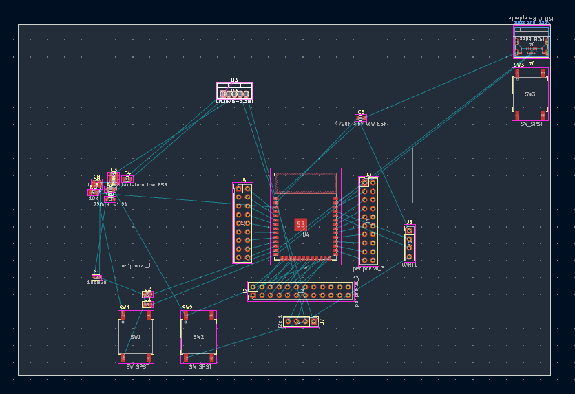
PCB Design Process in KiCAD
Moving from the schematic to the PCB
Introduction
I don't have anything new here,but for the time being, please enjoy this old video I made about the process:
Call To Action
This tutorial is part of a bigger course called "Intelligent Product Design", which I am building out at https://backpack.danaukes.com/course/intelligent_product_design/. Please pardon the dust as I build it out.
If you just want the tutorial, you're in the right spot. But, if you need a little more, such as live lectures, a discussion board, or a community of other students, consider enrolling once the course opens. For now, please feel free to explore https://backpack.danaukes.com.